Supply Voltage Range
0.7 V to 3.6 V
Low RON
9.0 mΩ Typ
IOUTMax
4 A
Ultra-Low IQ
5.6 μA Typ at 0.7 VIN ; 3.8 μA Typ at 0.8 VIN ; 8.8 μA Typ at 3.6 VIN
Ultra-Low ISD
14 nA Typ @ 3.6 VIN
Controlled VOUT Turn-on Time
111 μs at 0.7 VIN ; 113 μs at 0.8 VIN ;87 μs at 3.6 VIN
Internal EN Pull-Down Resistor
Integrated Output Discharge Switch
Reverse Current Blocking Protection When Disabled
Operating Temperature Range
- 40 °C to 105 °C
HBM: 8 kV, CDM: 2 kV
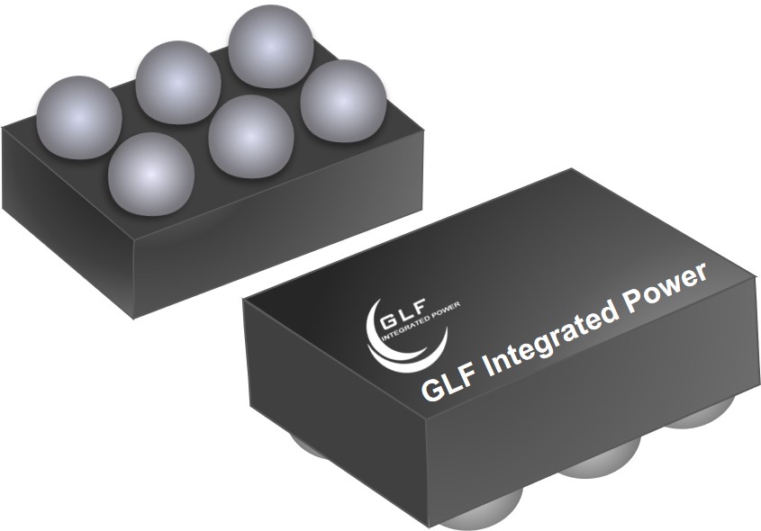
0.97 mm x 1.47 mm x 0.55 mm, 6 Bumps Wafer Level Chip Scale Package
The GLF72525 Load Switch is a fully integrated 4 A NMOS load switch with IQSmartTM advanced technology. The device is targeted for the mobile computing and data storage markets as a high performance solution for load switch applications.
The GLF72525 has a constant low on-resistance of 9.0 mΩ at the full input voltage range. The fixed rise time helps prevent undesirable inrush current when turned on and the internal EN pin pulldown resistor ensures the device remains in the shutdown mode when disabled. In shutdown mode the GLF72525 draws only 14 nA typical at 3.6 V input supply voltage.
The GLF72525 features a reverse current blocking protection. When the GLF72525 is disabled, it prevents reverse current flowing from the output to the input source.
The GLF72525 is available in a wafer level chip scale package (WLCSP) measuring 0.97 mm x 1.47 mm x 0.55 mm with a 0.5 mm pitch. This allows the user to save board space and increase cost savings.