Ultra-Low ISD
7 nA Typ @ 3.6VBAT
ltra-Low IQ
3 nA Typ @ 3.6VBAT
Low RON
31 mΩ Typ @ 3.6VBAT
IOUT Max
2A
Wide Input Range
1.5V to 5.5V 6Vabs max
Deep Sleep Mode by /SRO and OFF Pins Disconnect the downstream system from the battery source
Integrated Delay Time(Hold Time) to Deep Sleep
7S
Turn-Off Delay Time
7S
Controlled Output Rise Time
1ms at 3.6VBAT
Integrated Output Discharge Switch When Disabled
Operating Temperature Range
-40 to 85°C
HBM / CDM
6kV / 2kV
Ultra-Small
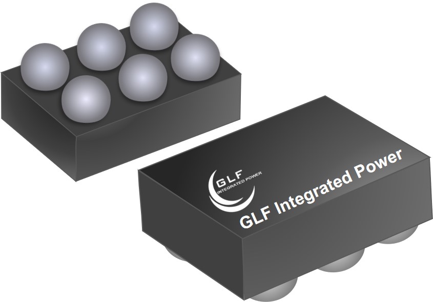
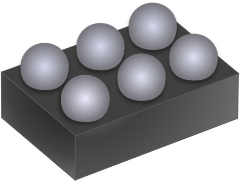
0.97mm x 1.47mm x 0.55mm
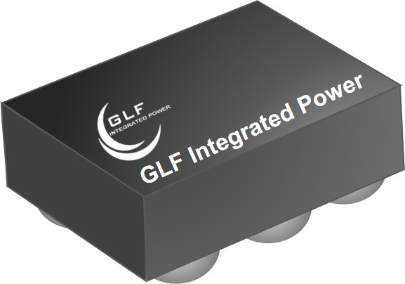
Ultra-Thin on GLF76321T
0.35mm Typ., 0.4mm Max.
The GLF76321 / GLF76321T is an ultra-thin, ultra-efficient IQSmartTM load switch with an integrated deepsleep timer for wearables and IoT devices.
The /SRO pin enables a whole system to enter ultradeep sleep power conservation mode by disconnecting the system from the battery charge, with ultra-low standby current of 7nA typical. With the switch placed between a battery and system, this switch can help to significantly extend system battery life in mobile devices during shipping or periods of extended off time.
The part supports two methods for entering the deep sleep: supporting both user and interrupt initiated events. Deep sleep can be initiated or exited by either holding the SRO pin low for a predefined delay time (ideal for user control) or by providing a rising edge signal to the OFF pin (ideal for logic or interrupt control).
To exit the deep sleep, the user can hold down the /SRO pin to ground for 1.3 seconds, or simply connect a charger adapter to trigger the Wake pin.
The GLF76321 / GLF76321T helps to reduce power consumption with the best in class RON and a breakthrough on state IQ of only 3nA typical when the switch is on.
The GLF76321 / GLF76321T integrated 1ms slew rate control can also enhance system reliability by mitigating bus voltage swings during switching events. Where uncontrolled switching can generate high inrush currents that result in voltage droop and/or bus reset events, the GLF slew rate control specifically limits inrush currents during turn-on to minimize voltage droop. The output discharge functions makes output voltage off quickly during the reset period.
The GLF76321 is available in 0.97mm x 1.47mm x 0.55mm wafer level chip scale package (WLCSP).
The GLF76321T is ultra-thin: 0.35mm Typ, 0.4mm Max